EasyEDA’s Gerber viewer for beginners and experts
 Few months ago, we had published an article about EasyEDA and described about its features. We see EasyEDA as one stop solution for all the PCB design and manufacturing processes. Check out the previous article about EasyEDA.
EasyEDA has been providing most of the services related to PCB/circuit design and manufacturing to its customers. The only thing missing was a Gerber viewer which has also been fulfilled recently. Check out EasyEDA’s Gerber Viewer.
We recently tested its Gerber viewer and noticed some exciting features that are rarely available on other Gerber viewers. Here are the 4 points that make EasyEDA’s Gerber viewer a complete solution for visualizing the layers of PCB.
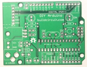
- True Visualization of your PCB: When we design a PCB, we would want to see how it may appear after it is manufactured. Professionals might have different software to visualize what they have designed. But, novices and beginners may not have access to such software and may not know which software feature would display the right layer of the PCB. For example, people using Eagle generally use preset *.CAM file for generating Gerbers and most of us don’t know which files mean which layer. We simply send the Gerber to the manufacturer and they decide which files to use for manufacturing our PCB. However, as an electronics enthusiast, we would want know the significance of each file that is generated by the CAM processor. We have noticed that EasyEDA’s Gerber viewer offers the feature of true visualization of different layers and we can literally see the image of the PCB that we would expect after it is manufactured.
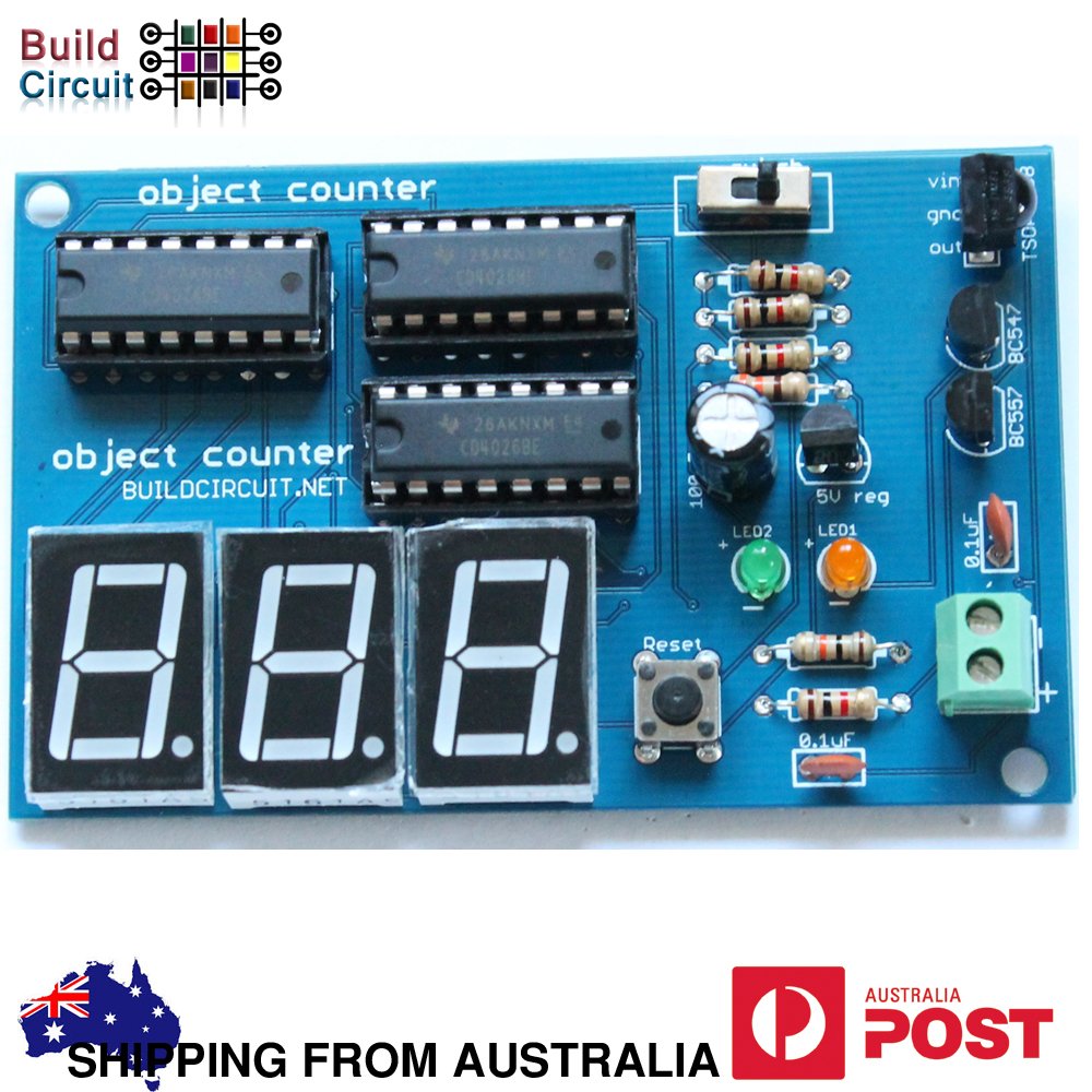
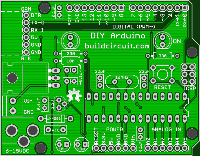
The images below show the real PCB(on the left) and the image from the Gerber viewer.
You can see more images on this article: Viewing BuildCircuit’s Gerber Files on EasyEDA Gerber Viewer
2. User friendly: The Gerber Viewer is highly user friendly. A beginner PCB designer who does not know about different layers of PCB can also guess, see and understand the significance of different Gerber files. You can choose different colors for PCB and surface finish metals (Gold or Silver). You can save the image and share with your team members and friends. Image magnification and reassignment of PCB layers are also noticeable features of the viewer. In addition to this, EasyEDA gives an overview of common mistakes that we may commit while extracting Gerber files.
3. Supports Gerber files from different PCB design software: We have tested the Gerber viewer with the files generated from EagleCad’s CAM processor and the results were excellent. You can try the viewer from other software as well and it should be compatible with the files generated by any software. Tutorials links for extracting Gerber files from Altium, Eagle, Diptrace and KiCad have been given on gerber viewer page.
4. Additional support from EasyEDA for correcting Gerber: EasyEDA is a cloud based circuit design tool to help designers move from idea to manufactured prototype by providing comprehensive data and collaboration tools for electronic design. It is suitable for all users spanning from hobbyists to engineers. EasyEDA has been established to integrate most of the aspects of electronics. As we start from our kit idea from schematic or circuit design to manufacturing, we come across several phases and EasyEDA addresses most of those phases. When we are in the Gerber viewing phase of our product development cycle, EasyEDA is there to support us when there is any error in the design file. You can submit a bug report to its support team and get the required help.
Additionally, on the Gerber viewer page you will also get an overview of common mistakes that we may commit while generating the Gerber files. All of your Gerbers are unlisted. They are not shared with anyone. If you are concerned about this, once you have viewed them, you can remove your Gerbers from the server.

Watch the following video to see how EasyEDA’s Gerber Viewer works:
Related Article: Viewing BuildCircuit’s Gerber Files on EasyEDA Gerber Viewer

